166 AstraPIO
166 : AstraPIO
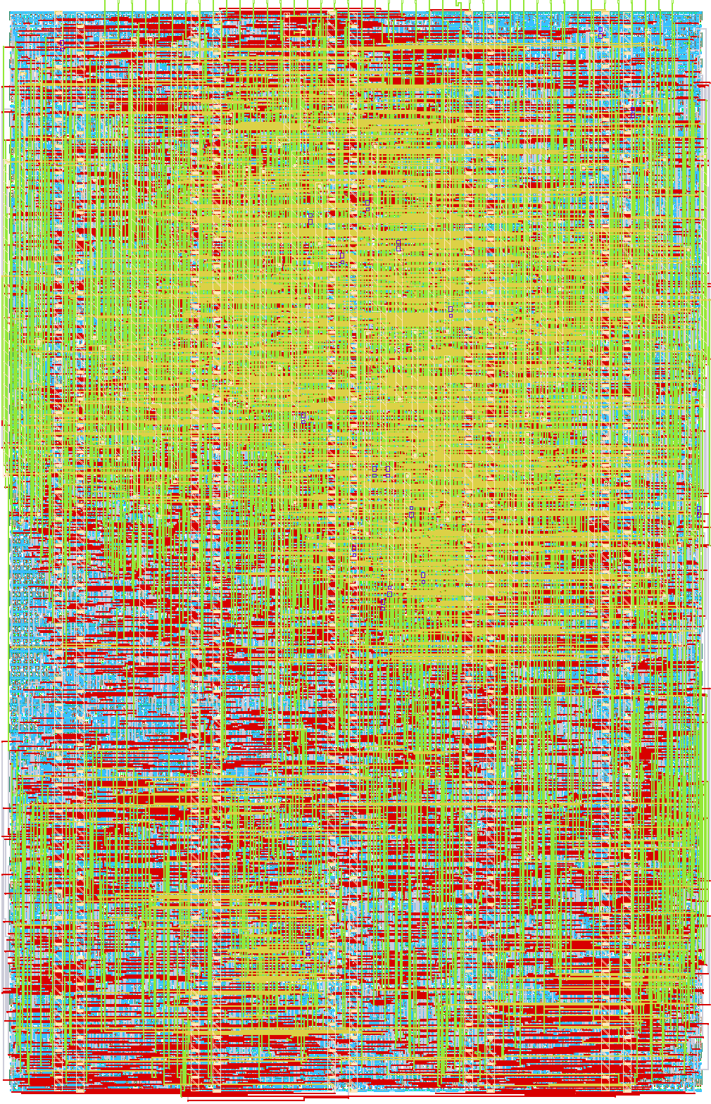
- Author: Fabien
- Description: Programmable PIO and autonomous timed I/O coprocessor (ABI 5)
- GitHub repository
- Open in 3D viewer
- Open in Tiny Tapeout Explorer
- Clock: 50000000 Hz
AstraPIO
Programmable digital I/O coprocessor with a host SPI interface.
How it works
AstraPIO combines a programmable PIO interpreter with an independent timed pulse engine. The host configures both blocks and exchanges data over SPI; individual I/O transitions are handled by the ASIC.
The PIO provides 16 ten-bit instructions, an eight-bit accumulator, a four-bit
loop counter and two-byte TX and RX FIFOs. An instruction slot occurs every
four ASIC clocks. Instructions support GPIO direction and output control,
input sampling, conditional branches, loops, delays and host events.
PULL and PUSH wait when the corresponding FIFO cannot transfer data.
The timed engine samples pulse-width-coded input bits after a programmable delay. It can capture a 1 to 24-bit prefix, regenerate the stream, and replace the prefix with a host-supplied value. Updates take effect atomically at a qualified frame boundary. The remaining bits are regenerated without a frame buffer. The PIO and timed engine can run concurrently on separate outputs.
Typical applications include GPIO sequencing, simple serial transmitters and pulse-stream processing. Live WS2812 prefix replacement is described in a separate application note; AstraPIO is a general-purpose I/O device.
Host interface
SPI mode 0, MSB first, with exactly 32 clocks per CS assertion:
command byte (0x02 write, 0x03 read), register address byte, then 16 data bits.
On reads, only the last two received bytes contain register data.
SCK high and low periods, plus CS setup, hold and inactive gaps, must each be at least six ASIC clocks. At CLK = 50 MHz this is 120 ns. MISO remains driven with CS inactive: use a dedicated MISO input or external bus isolation. IRQ is an active-high level shared by data-ready and error sources.
How to test
- Select the design, supply CLK, keep host CS high and SCK low, then apply and release reset. Allow at least five CLK cycles in reset and five after release as a functional startup sequence.
- Read
0x00,0x01,0x02and0x0F: expect0x5049,0x0500,0x0001and0x1002. - With the PIO stopped, load consecutive instructions at
0x40through0x4Fand read them back. Each word must fit in ten bits. Assemble with--abi 5. - Set the output mask at
0x10, entry PC at0x11, then write1to RUN at0x03. Read error and FIFO status registers during use.
The timed engine has its own register page at 0x60 through 0x6C, with
identity 0x5449 and version 0x0118. Configure it disabled. Reserve its
output separately from the PIO mask, then enable the selected mode.
Pin use
| Ports | Function |
|---|---|
ui_in[0], [1], [2] |
Host SCK, MOSI, active-low CS |
ui_in[3] through [7] |
Application input indices I8 through I12 |
uo_out[0], [1] |
Host MISO, active-high IRQ |
uo_out[2] through [7] |
Application output indices O8 through O13 |
uio[0] through [7] |
Bidirectional application pins I0/O0 through I7/O7 |
The eight bidirectional pins are included in both the 13-input and 14-output logical index spaces. Each output can belong to only one block. Reset or deselection forces output values low and disables the bidirectional drivers. Stopping the PIO retains its output levels and directions.
External hardware
A microcontroller with an SPI master, a clock source and the application circuit. A portable C driver is provided; the board-specific SPI transport must serialize accesses and respect the CS timing. Program and configuration are volatile and must be loaded after global reset.
Check the delivered IHP carrier board for physical pin mapping, supply rails, logic levels and level translation. Logical port names are not package pin numbers. No direct 5 V compatibility is specified.
Documentation
The interface described here is ABI 5. The reference clock is 50 MHz; all programmable delays scale with CLK. Functional simulation does not constitute electrical characterization or board-level qualification.
IO
| # | Input | Output | Bidirectional |
|---|---|---|---|
| 0 | HOST_SCK | HOST_MISO | PIO_IO0 |
| 1 | HOST_MOSI | HOST_IRQ | PIO_IO1 |
| 2 | HOST_CS_N | PIO_OUT0 | PIO_IO2 |
| 3 | PIO_IN0 | PIO_OUT1 | PIO_IO3 |
| 4 | PIO_IN1 | PIO_OUT2 | PIO_IO4 |
| 5 | PIO_IN2 | PIO_OUT3 | PIO_IO5 |
| 6 | PIO_IN3 | PIO_OUT4 | PIO_IO6 |
| 7 | PIO_IN4 | PIO_OUT5 | PIO_IO7 |