617 Simple comparator + 2 DACs analog layout in a 1x1 tile
617 : Simple comparator + 2 DACs analog layout in a 1x1 tile
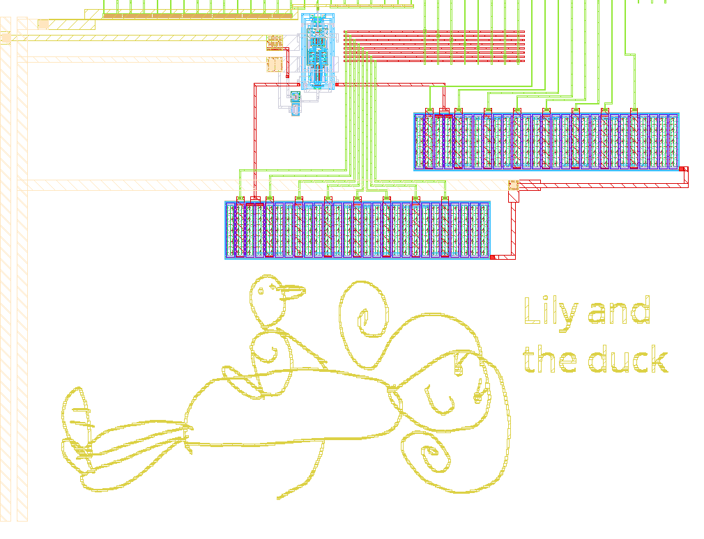
- Author: algofoogle (Anton Maurovic)
- Description: IHP sg13g2 custom layout analog experiments in a regular TT 1x1 digital tile
- GitHub repository
- Open in 3D viewer
- Open in Tiny Tapeout Explorer
- Clock: 0 Hz
What is this project?
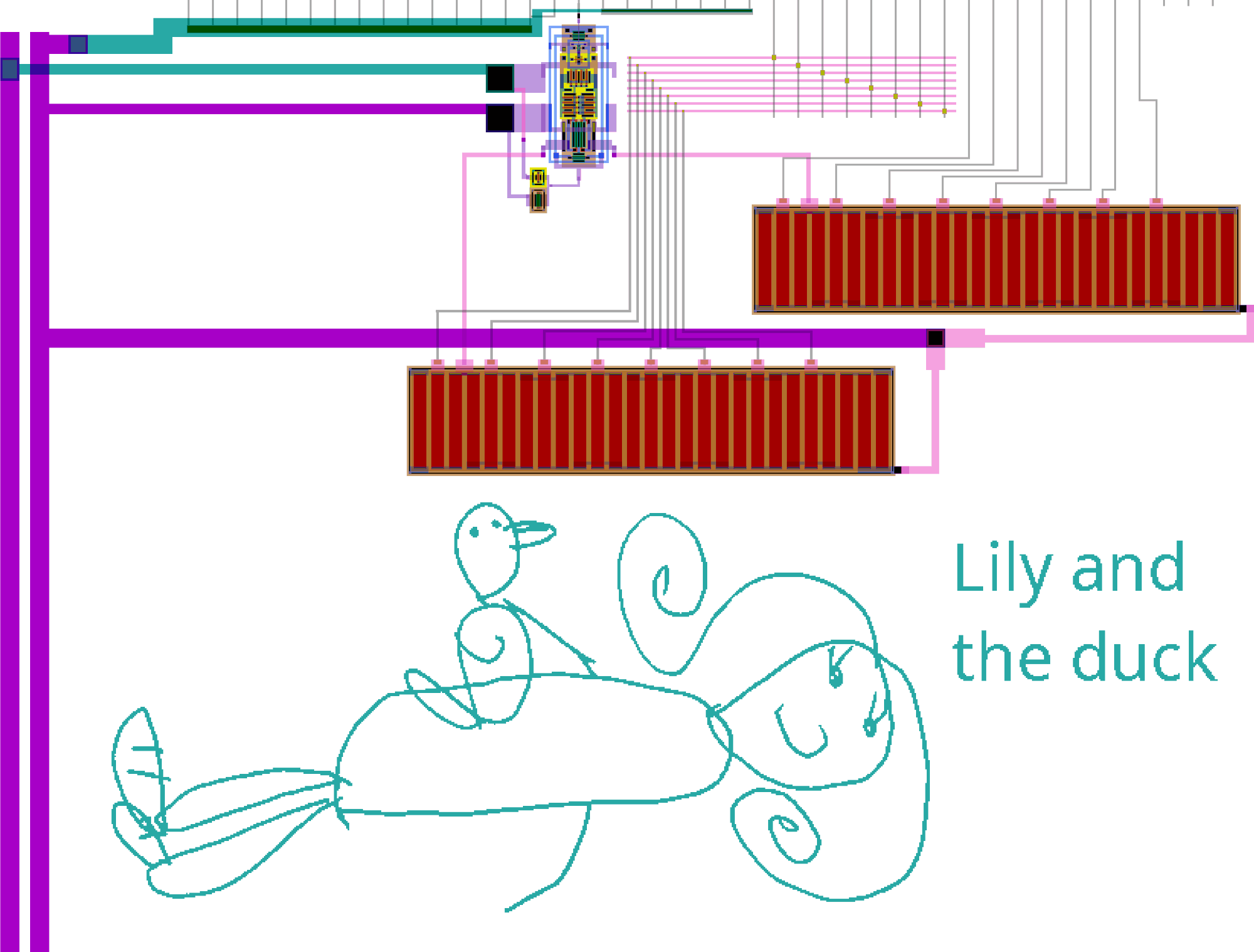
This custom GDS layout uses Tiny Tapeout 1x1 tile space normally intended for digital-only projects, and implements 4 analog elements that provide a basic testing harness for a simple analog comparator. ui_in and uio_in (the bidirectional pins) respectively drive DACs to set two voltages to be compared, while comparator_out provides the digital comparison result: high if ui_in is greater than uio_in, or low if uio_in is greater.
The output is estimated to be reasonably accurate for DAC codes 64..213 (0.3V to 1.0V).
The GDS art in the bottom half is a drawing done by my daugther when she was 4.
How does it work?
Overview
This design can only interface with the outside world using digital IOs (since it is using a Tiny Tapeout 1x1 tile which has no analog ports), and since it is an analog experiment it needs a way to control analog values internally from digital inputs.
I used a simple 8-bit R2R DAC design and created two instances of it: one driven by inputs on ui_in (aka pdac) and the other on uio_in (aka ndac). These connect to the positive and negative inputs of the main target of this design: A simple analog comparator. It amplifies the difference between the positive and negative inputs to produce a digital output (comparator_out) which is high when the selected positive value is greater than the negative value, and low otherwise.
Analog blocks
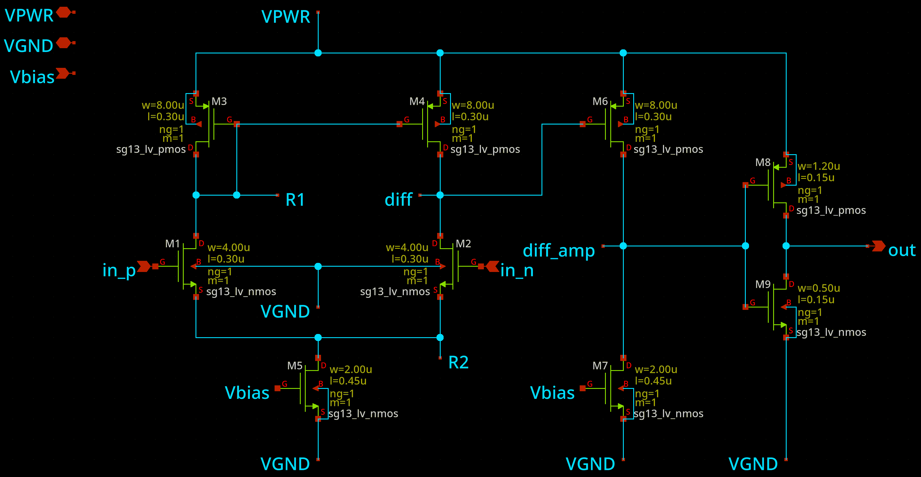
The comparator is a simple design:
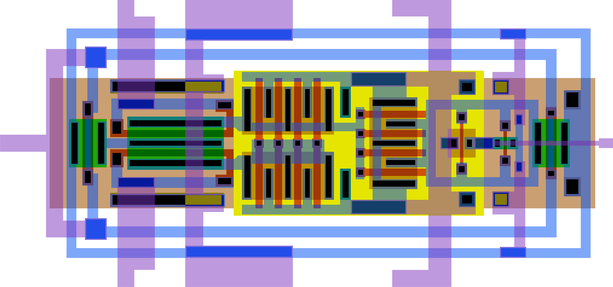
With its layout I tried to use a sensible symmetry/matching approach:
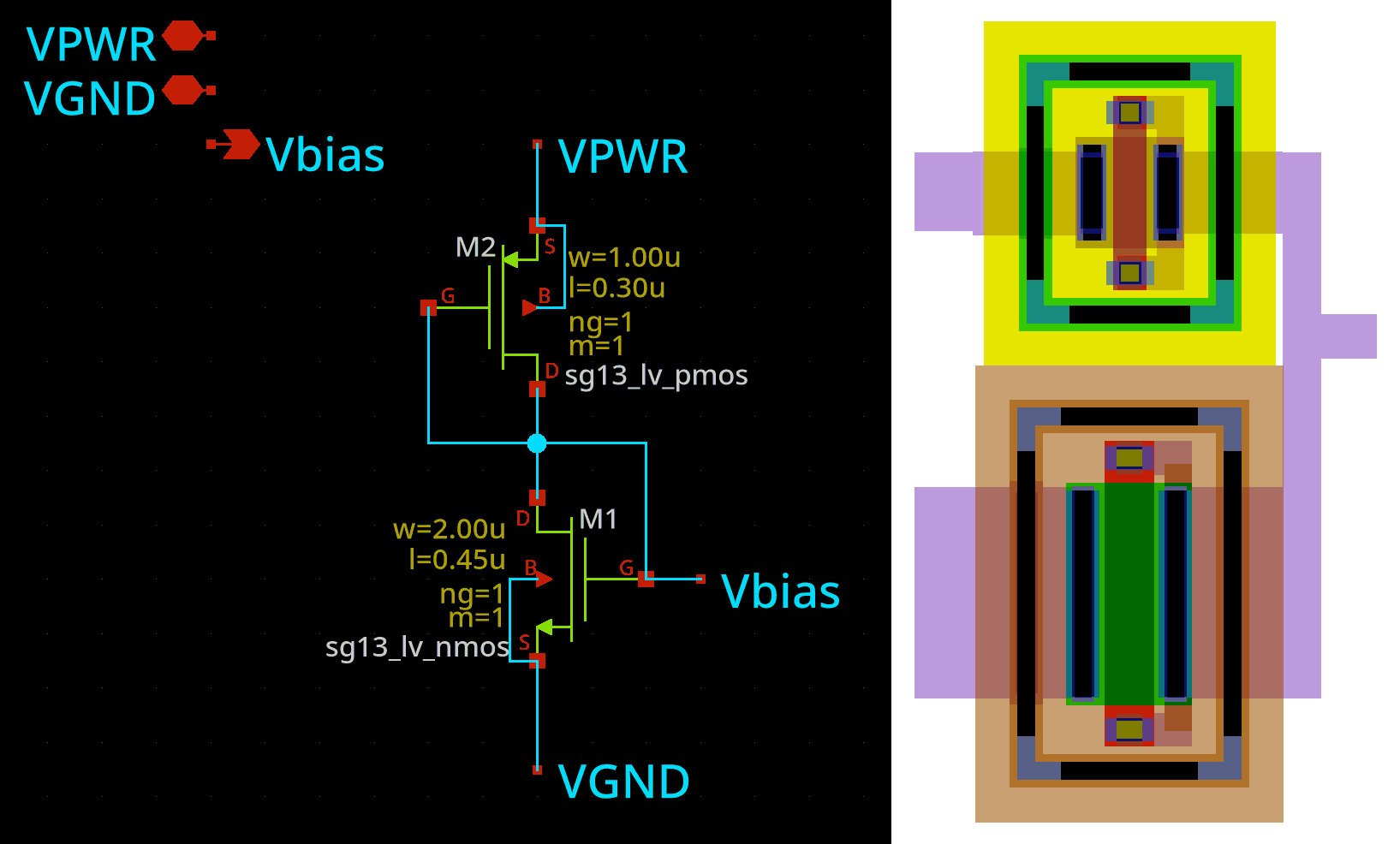
The comparator's M5 transistor provides the tail current, and it is matched with M7. The gate reference voltage for these is created by the naively simple Vbias circuit (for which there are probably many better designs I could have used but this is adequate for this very simple design, I think):
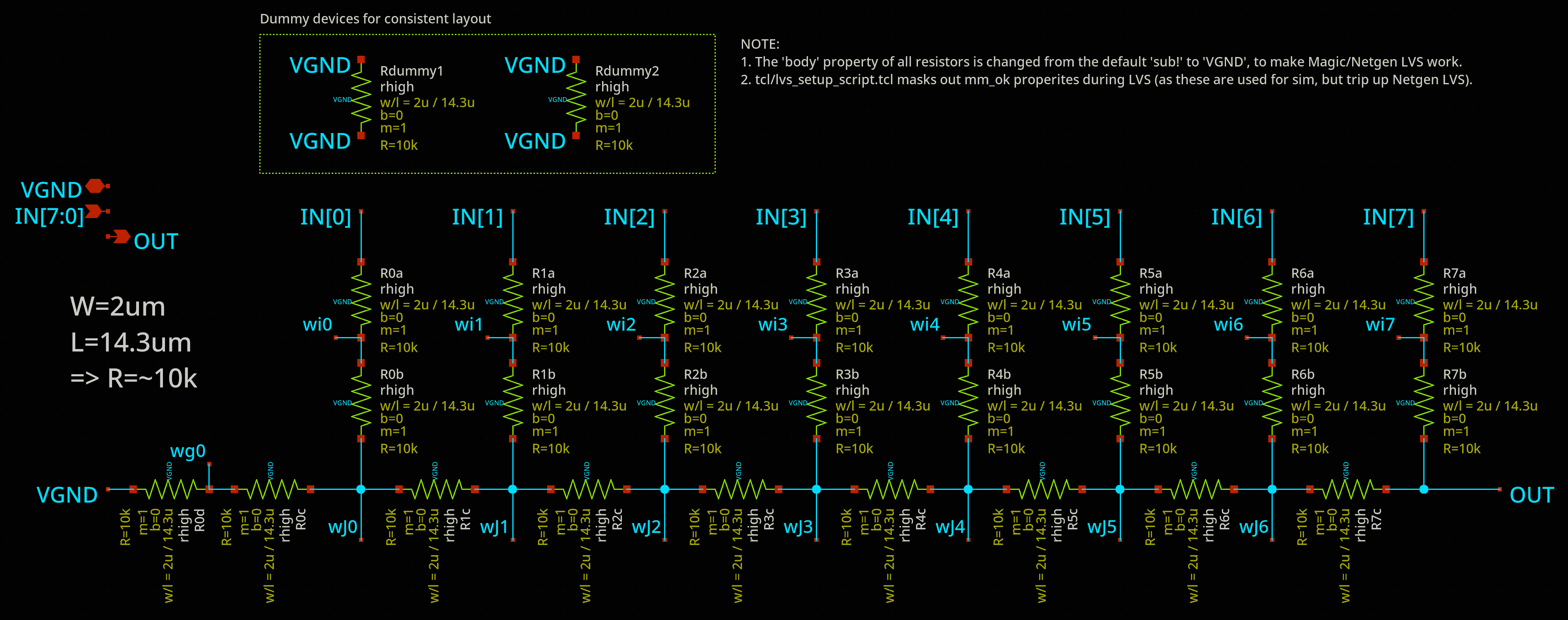
The comparator's positive ("in_p") and negative ("in_n") inputs are analog voltages that can be set to anything in the range of 0 to 1.2V (with a step size of ~4.7mV per each of the 256 DAC input codes). The two DACs are a simple R2R design with a target R=10k:
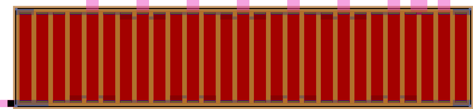
The layout attempts to respect matching, including the use of a dummy resistor at each end:
Performance
Due to having very little time to work on this, I can't say that I'd expect it to perform very well in silicon and across PVT. Nevertheless, parasitic extraction and simulation indicates it should be able to compare voltages reasonably well in the range of 0.3V to 1.0V, to an accuracy of 5mV or better (hopefully able to discriminate DAC inputs that are only 1 code apart).
How to test
This design doesn't use the clk or rst_n pins. The bidirectional pins are permanently configured as inputs.
Try comparing values on ui_in with those on uio_in -- if ui_in is greater, uo_out[7] should go high. Note that the comparator is generally considered to be reliable for voltages in the range of 0.3V to 1.0V internally (DAC codes 64..213). Voltages in range of about 0.45V to 0.85V should give the fastest response (on the order of 2-3ns) while codes nearer 0.3V and 1.0V might respond much slower (on the order of 10-20ns).
External hardware
Not much is needed to test this. The Tiny Tapeout demo board, when configured to drive the bidirectional pins, is quite an easy way to assert the ui_in and uio_in binary values to the DACs, and uo_out[7] (comparator_out) can then be observed to see the result.
Besides that, you might want an oscilloscope to measure the output in response time with respect to changing inputs.
IO
| # | Input | Output | Bidirectional |
|---|---|---|---|
| 0 | pdac[0] | ndac[0] | |
| 1 | pdac[1] | ndac[1] | |
| 2 | pdac[2] | ndac[2] | |
| 3 | pdac[3] | ndac[3] | |
| 4 | pdac[4] | ndac[4] | |
| 5 | pdac[5] | ndac[5] | |
| 6 | pdac[6] | ndac[6] | |
| 7 | pdac[7] | comparator_out | ndac[7] |