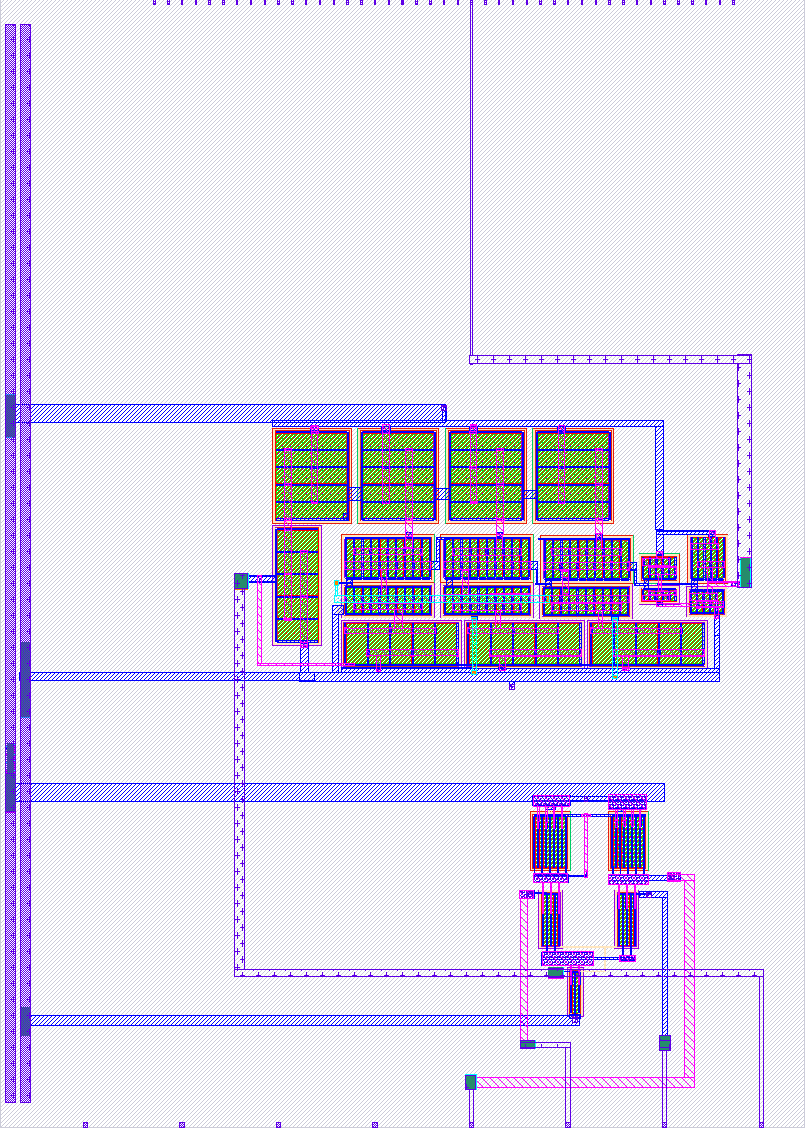
267 Ring oscillator VCO and Differential Amplifier
267 : Ring oscillator VCO and Differential Amplifier
- Author: Vipul Sharma
- Description: Current-controlled analog VCO
- GitHub repository
- Open in 3D viewer
- Clock: 0 Hz
How it works
This tile integrates two independent analog designs in the SkyWater Sky130 130 nm PDK, sharing a single DC bias/control pin (ua[0]) due to the 4-analog-pin Tiny Tapeout limit. Both circuits are permanently powered from VDD = 1.8 V and are tested through separate analog/digital pins.
Design 1 — 3-Stage Current-Starved Ring Oscillator VCO
The VCO core is a 3-stage current-starved ring oscillator with PMOS current-source loads and NMOS tail-current sources, all gated by a single control voltage Vctrl. Varying Vctrl starves or boosts the per-stage current and directly tunes the oscillation frequency. A two-stage CMOS output buffer drives the digital output pin to rail-to-rail and isolates the core from external loading. Measured tuning range: ~5.27 MHz at Vctrl = 0.7 V to ~57.57 MHz at Vctrl = 1.7 V.
How to test:
- Apply VDD = 1.8 V.
- Apply the DC control voltage
Vctrlonua[0](shared bias pin) and sweep it from 0.7 V to 1.7 V in 0.1 V steps. - Observe the buffered square-wave output on
uo[0]with a scope or frequency counter; expected range ~5 MHz to ~57 MHz. - Plot frequency vs.
Vctrland compare against the TT/27 °C characterization.
Design 2 — 5T Differential Amplifier with Active Current-Mirror Load
The diff-amp is a 5-transistor NMOS-input pair (M1, M2) with a PMOS current-mirror active load (M4, M5) and an NMOS tail-current source (M3) biased by Vbias. The single-ended output is taken at the drain of M2/M5. It amplifies the small-signal difference between Vin+ and Vin− around a 0.9 V common-mode level.
How to test:
- Apply VDD = 1.8 V.
- Apply DC
Vbias= 0.9 V onua[0](shared with the VCOVctrl; this same DC level biases the tail source). - Apply
Vin+onua[1]— e.g., 0.9 V DC + 10 mV / 1 MHz sine. - Apply
Vin−onua[2]— 0.9 V DC reference. - Observe the amplified single-ended output
Voutonua[3].
Pin summary
| Pin | Function |
|---|---|
ua[0] |
Shared DC input — VCO Vctrl and Diff-Amp Vbias |
ua[1] |
Diff-Amp Vin+ |
ua[2] |
Diff-Amp Vin− |
ua[3] |
Diff-Amp Vout |
uo[0] |
VCO buffered digital frequency output |
Bench testing with Digilent Analog Discovery 3
The Analog Discovery 3 (AD3) provides everything needed to characterize both circuits from a single USB-C connection: a programmable supply V+ (0–5 V, used for VDD), two arbitrary waveform generators W1/W2 (±5 V), and two scope channels 1+/1−, 2+/2− (14-bit, 30 MHz BW). All measurements share the AD3 ground (⏚) with the chip ground. Use the WaveForms software (Supplies, WaveGen, Scope, Network Analyzer instruments).
Common setup (both tests):
V+→ chip VDD, set to 1.8 V, enable in Supplies.- AD3
⏚→ chip GND. - Keep leads short and add a 100 nF decoupling cap from VDD to GND near the chip.
Testing the Ring Oscillator VCO with AD3
| AD3 channel | Connect to | Setting |
|---|---|---|
V+ |
VDD | 1.8 V DC |
W1 |
ua[0] (Vctrl) |
DC, swept from 0.7 V → 1.7 V in 0.1 V steps |
Scope 1+ |
uo[0] (VCO out) |
AC or DC coupled, 1 V/div |
Scope 1− |
GND | — |
Procedure:
- In WaveGen, set
W1to DC mode, offset 0.7 V, enable output. - In Scope, set timebase to ~50 ns/div; enable the built-in Measurements → Frequency readout.
- Step
W1offset from 0.7 V to 1.7 V; log frequency at each step. Expected: ~5 MHz → ~57 MHz. - (Optional) Automate the sweep using the WaveForms Script tool to record a full Vctrl-vs-frequency table.
Note: AD3 scope analog bandwidth is 30 MHz. For VCO frequencies > 30 MHz (Vctrl > ~1.2 V), use the Logic Analyzer input (
DIO 0) tied touo[0]and enable the Frequency counter — DIO sampling is 125 MS/s and resolves the full ~57 MHz range cleanly.
Testing the Differential Amplifier with AD3
| AD3 channel | Connect to | Setting |
|---|---|---|
V+ |
VDD | 1.8 V DC |
W1 |
ua[1] (Vin+) |
Sine, 0.9 V offset, 10 mV amplitude, 1 MHz |
W2 |
ua[2] (Vin−) and ua[0] (Vbias) (tied together externally) |
DC, 0.9 V |
Scope 1+ |
ua[1] (Vin+) |
AC coupled, 10 mV/div |
Scope 2+ |
ua[3] (Vout) |
AC coupled, 50–100 mV/div |
Scope 1−, 2− |
GND | — |
Procedure:
- In Supplies, enable
V+= 1.8 V. - In WaveGen:
W1= Sine, 1 MHz, 10 mV amplitude, 0.9 V offset;W2= DC 0.9 V. Enable both. - In Scope: capture Ch1 (input) and Ch2 (output) on the same timebase (~200 ns/div). Compute small-signal gain Av =
Vout_pp / Vin_pp. - For an AC sweep, switch to the Network Analyzer instrument: source =
W1intoVin+, reference = Scope Ch1 onVin+, response = Scope Ch2 onVout. Sweep 100 Hz → 10 MHz to obtain the Bode magnitude/phase response (gain, −3 dB bandwidth, GBW).
Note: Since
VbiasandVin−both want 0.9 V DC, jumper them to a singleW2channel. AD3 has only two AWG outputs, so this tie is what makes a full 3-voltage diff-amp test fit on the instrument.
External hardware
No external hardware is required beyond the Analog Discovery 3 (or any equivalent DC supply + function generator + oscilloscope/frequency counter). A small breakout PCB or jumper wires are needed to route AD3 channels to the chip's analog (ua[0..3]) and digital (uo[0]) pins.
IO
| # | Input | Output | Bidirectional |
|---|---|---|---|
| 0 | VCO Frequency output | ||
| 1 | |||
| 2 | |||
| 3 | |||
| 4 | |||
| 5 | |||
| 6 | |||
| 7 |
Analog pins
ua | PCB Pin | Internal index | Description |
|---|---|---|---|
| 0 | B0 | 6 | Shared Control/Bias |
| 1 | B1 | 7 | Diff-Amp In+ |
| 2 | B3 | 9 | Diff-Amp In- |
| 3 | B2 | 8 | Diff-Amp Out |