581 Register bank accessible through SPI and I2C
581 : Register bank accessible through SPI and I2C
- Author: Caio Alonso da Costa
- Description: Register bank accessible through SPI and I2C
- GitHub repository
- Open in 3D viewer
- Clock: 50000000 Hz
- Feedback: ✅ 1
How it works
Register bank accessible throught two different serial interfaces: SPI and I2C. Use digital input to select prefered interface.
Digital input ui_in[7] = 0 selects SPI and ui_in[7] = 1 selects I2C.
Block diagram
                +----------------------------------------+
                |                                        |
                |   +-----------+        +-----------+   |
SPI Pins <----> |   | SPI Slave |        | I2C Slave |   | <----> I2C Pins
                |   | Interface |        | Interface |   |
                |   +-----+-----+        +-----+-----+   |
                |         ^                    ^         |
                |         |                    |         |
                |         |                    |         |
                |         v                    v         |
                |      +--+--------------------+--+      |
                |      |        Bus Arbiter       |      |
                |      +-------------+------------+      |
                |                    ^                   |
                |                    |  Internal         |
                |                    |  Register         |
                |                    |  Access Bus       |
                |                    v                   |
                |      +-------------+------------+      |
                |      |       Register Bank      |      |
                |      |                          |      |
                |      |   +------------------+   |      |
                |      |   |       REG0       |---|------|------> 7 segments display
                |      |   +------------------+   |      |
                |      |                          |      |
                |      |   +------------------+   |      |
                |      |   |       REG1       |   |      |
                |      |   +------------------+   |      |
                |      |            ...           |      |
                |      |   +------------------+   |      |
                |      |   |       REG14      |   |      |
                |      |   +------------------+   |      |
                |      |                          |      |
                |      |   +------------------+   |      |
                |      |   |       REG15      |   |      |
                |      |   +------------------+   |      |
                |      +--------------------------+      |
                |                                        |
                +----------------------------------------+
There are 8 read/write 8 bit registers and 8 read only 8 bit registers.
Address 0 (first byte in read/write register space) drives the 7 segment display.
SPI peripheral design based on https://github.com/calonso88/tt07_alu_74181
See that design's docs for information about the SPI peripheral.
Small improvement done on the spi_peripheral module. There used to be two buffer counters (one for RX and one for TX). Since the counters are not used together, it was possible to remove one of them and use a single buffer counter. This has reduced 4 flip flops in total and some combinatorial logic as well.
Added logic to control driver for MISO. On previous submissions of this design, the MISO was always driven. Logic has been added to put MISO into high impedance when CS_N is driven high. Due to a 2-stage synchronizer, the MISO goes to high impedance after 2 clock cycles.
I2C peripheral design based on https://github.com/sanojn/tt06_ttrpg_dice
See that design's docs for information about the I2C peripheral.
Protocol specification
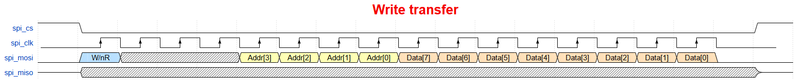
SPI Write (CPOL = 0, CPHA = 0)
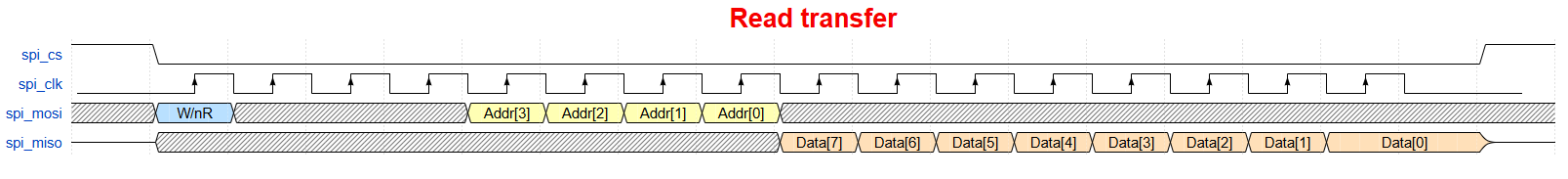
SPI Read (CPOL = 0, CPHA = 0)
I2C Frame

Register Map
| Offset | Name | Access | Reset | Description |
|---|---|---|---|---|
| 0x00 | REG0 | R/W | 0x00 | Controls 7 segmets display on demoboard |
| 0x01 | REG1 | R/W | 0x00 | General prupose register |
| 0x02 | REG2 | R/W | 0x00 | General prupose register |
| 0x03 | REG3 | R/W | 0x00 | General prupose register |
| 0x04 | REG4 | R/W | 0x00 | General prupose register |
| 0x05 | REG5 | R/W | 0x00 | General prupose register |
| 0x06 | REG6 | R/W | 0x00 | General prupose register |
| 0x07 | REG7 | R/W | 0x00 | General prupose register |
| 0x08 | REG8 | RO | 0xCA | Constant ID Code 1 |
| 0x09 | REG9 | RO | 0x10 | Constant ID Code 2 |
| 0x0A | REG10 | RO | 0xAA | Constant ID Code 3 |
| 0x0B | REG11 | RO | 0x55 | Constant ID Code 4 |
| 0x0C | REG12 | RO | 0xFF | Constant ID Code 5 |
| 0x0D | REG13 | RO | 0x00 | Constant ID Code 6 |
| 0x0E | REG14 | RO | 0xA5 | Constant ID Code 7 |
| 0x0F | REG15 | RO | 0x5A | Constant ID Code 8 |
How to test
SPI
Use SPI1 Master peripheral in RP2040 to start communication on SPI interface towards this design. Remember to configure the SPI mode using digital inputs [0] and [1] to high (if you'd like to have CPOL=1 and CPHA=1).
Example code to initialize SPI in REPL:
spi_miso = tt.pins.pin_uio3
spi_cs = tt.pins.pin_uio4
spi_clk = tt.pins.pin_uio5
spi_mosi = tt.pins.pin_uio6
spi_miso.init(spi_miso.IN, spi_miso.PULL_DOWN)
spi_cs.init(spi_cs.OUT)
spi_clk.init(spi_clk.OUT)
spi_mosi.init(spi_mosi.OUT)
spi = machine.SoftSPI(baudrate=10000, polarity=0, phase=0, bits=8, firstbit=machine.SPI.MSB, sck=spi_clk, mosi=spi_mosi, miso=spi_miso)
spi_cs(1)
Example code to write 0xF8 to address[0]:
spi_cs(0); spi.write(b'\x80\xF8'); spi_cs(1)
This should set the 7 segment LED to 0xF8 which will display "t."
Seg A - OFF, Seg B - OFF, Seg C - OFF, Seg D - ON, Seg E - ON, Seg F - ON, Seg G - ON, Seg DP - ON
Example code to read from address[0]:
spi_cs(0); spi.write(b'\x00'); spi.read(1); spi_cs(1)
The result should be 0xF8 or whatever you wrote to address[0].
I2C
Use I2C Master peripheral in RP2040 to start communication on I2C interface towards this design. Remember to configure the I2C address bits using the digital inputs [2], [3] and [4]. Example code below assumes that flex i2c address bits are configured to 0, i.e., configure digital inputs [2], [3] and [4] to 0. Configure digital input [7] to 1 to enable I2C to interface the register bank.
Example code to initialize I2C in REPL:
i2c_scl = tt.pins.pin_uio2
i2c_sda = tt.pins.pin_uio1
i2c = machine.SoftI2C(scl=i2c_scl, sda=i2c_sda, freq=100000)
Example code to write one byte value 0xF8 to address[0]. Write to i2c_addr 0x70, starting at memory addr 0, 1 byte (0xF8).
i2c.writeto_mem(112, 0, b'\xF8')
Example code to read one byte from address[0]. Read from i2c_addr 0x70, starting at memory addr 0, 1 byte.
i2c.readfrom_mem(112, 0, 1)
Example code to write four bytes to address[3-6]. Write to i2c_addr 0x70, starting at memory addr 3, 4 bytes (b'1234').
i2c.writeto_mem(112, 3, b'1234')
Example code to read five bytes from address[9-13]. Read from i2c_addr 0x70, starting at memory addr 9, 5 bytes.
i2c.readfrom_mem(112, 9, 5)
External hardware
You may need to use pull up resistors (2k2) on the i2c_sda and i2c_scl lines. Write to the first register to set the LEDs on the demoboard.
IO
| # | Input | Output | Bidirectional |
|---|---|---|---|
| 0 | cpol | spare[0] | |
| 1 | cpha | spare[1] | i2c_sda |
| 2 | i2c_addr[0] | spare[2] | i2c_scl |
| 3 | i2c_addr[1] | spare[3] | spi_miso |
| 4 | i2c_addr[2] | spare[4] | spi_cs_n |
| 5 | spare[5] | spi_clk | |
| 6 | spare[6] | spi_mosi | |
| 7 | peripheral selector (SPI=0/I2C=1) | spare[7] |
User feedback
- smunaut: Tested SPI access using instructions in the doc and checking other registers and all worked as expected. Also tested I2C register using instructions in the docs, except I configured Pico internal pull-ups on SDA/SCL and I was able to read-write registers as expected, including multi-read/write.